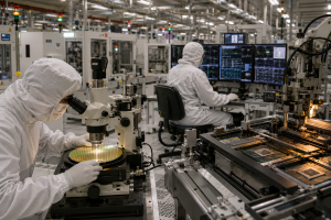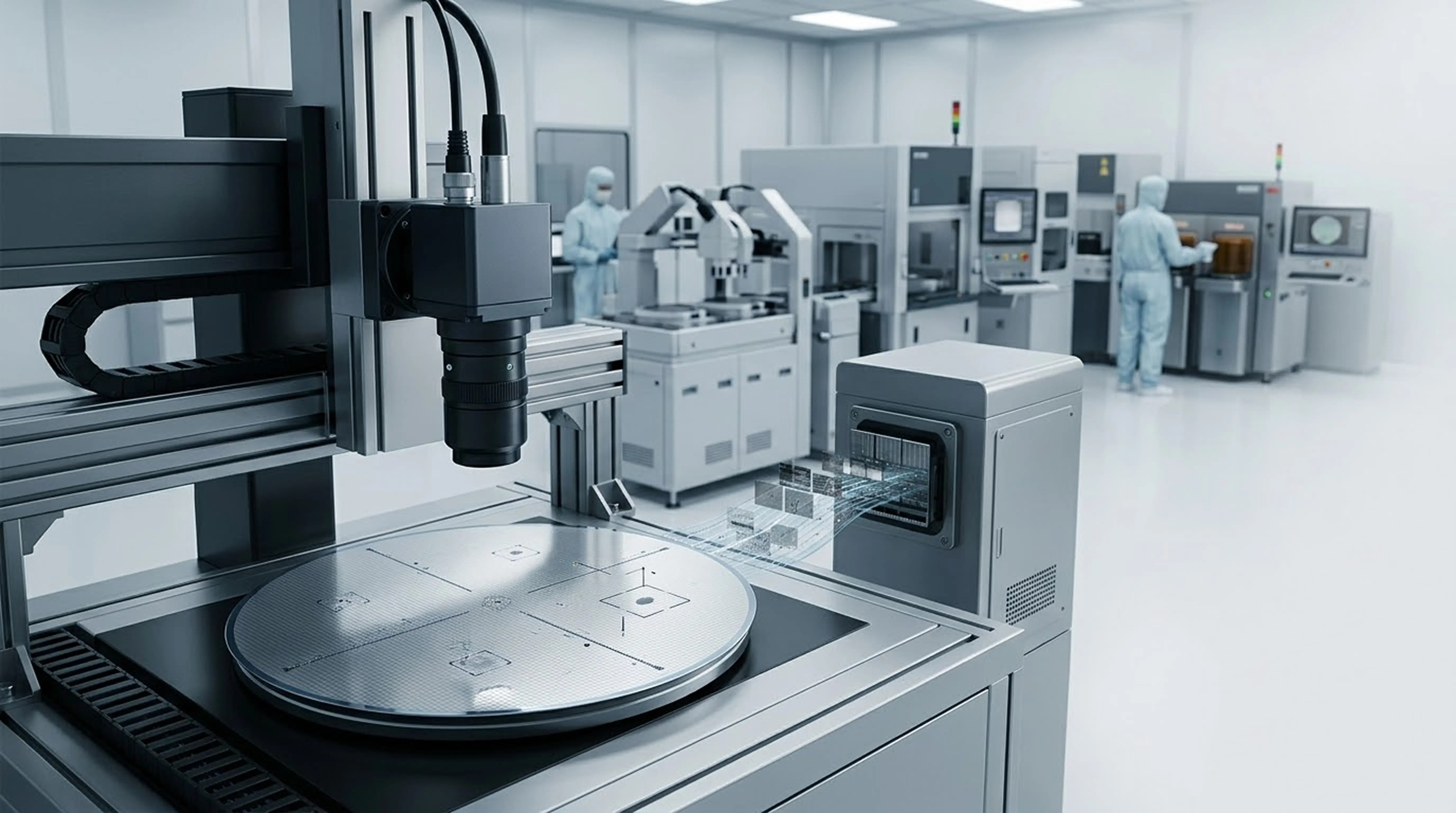
AI in semiconductor manufacturing is changing how modern fabs approach inspection, defect detection, quality control, and production data analysis. While most attention goes to AI models and computing power, the chips behind those systems have to be manufactured, inspected, tested, and packaged with extremely high precision.
That is where AI is becoming useful on the manufacturing floor.
From computer vision for defect detection to machine learning for predictive maintenance and edge AI for real-time inspection, manufacturers can use AI to turn large amounts of production data into faster, more informed decisions.
How AI Is Changing Semiconductor Manufacturing
Semiconductor production generates data at almost every stage of the process. Cameras capture inspection images, equipment produces sensor data, and manufacturing systems continuously record process conditions.
As chip designs, packaging methods, and production processes become more complex, making sense of this data becomes increasingly difficult.
AI can help by finding patterns in production data that may otherwise require extensive manual analysis. Depending on the application, this can support:
- Automated visual inspection
- Defect detection and classification
- Predictive maintenance
- Process monitoring
- Quality control
- Production optimization
The goal is not to replace manufacturing expertise. It is to give engineers better information at the point where decisions need to be made.
AI for Semiconductor Inspection
Inspection is one of the clearest applications of AI in semiconductor manufacturing.
A modern inspection system may capture thousands or millions of images and measurements during production. Reviewing all of that information manually is difficult to scale, particularly when defects can be extremely small or visually similar to normal process variation.
Computer vision can analyze inspection images and identify potential anomalies.
A typical workflow looks like this:
Image capture → AI analysis → Defect detection → Classification → Quality decision
AI can help distinguish between different types of defects, identify their location, and prioritize results for further investigation.
This matters because detecting an anomaly is only the first step. Manufacturing teams also need to understand what the anomaly is and whether it requires action.
Recent semiconductor-industry work demonstrates this direction. NVIDIA and TSMC announced the use of vision AI for automated defect inspection, while NVIDIA has also described AI-based approaches for wafer and die-level defect classification.
Computer Vision for Defect Detection
Computer vision gives manufacturing systems the ability to interpret visual information from cameras and inspection equipment.
In semiconductor environments, it can be applied to areas such as wafer inspection, packaging inspection, surface analysis, and other quality-control tasks.
A simplified inspection process is:
Why Inspection Systems Are Becoming Critical to Manufacturing Scalability
One of the less visible bottlenecks inside semiconductor manufacturing environments is inspection complexity.
Modern fabs generate enormous volumes of inspection data across:
- wafer fabrication
- lithography
- etching
- metrology
- bonding
- advanced packaging
- and final testing workflows
As production scales, inspection systems are generating growing numbers of anomalies, alerts, and defect classifications.
And that creates a major operational challenge:
false positives.
In many semiconductor environments, engineering teams spend substantial amounts of time reviewing anomalies that may not represent meaningful manufacturing defects at all.
Over time, excessive false positives can create:
- inspection bottlenecks
- slower review cycles
- operational fatigue
- inconsistent classifications
- delayed production decisions
- and increased manufacturing overhead
In high-volume production environments, even small inefficiencies in inspection workflows can scale into significant operational costs.
The issue is not simply detecting anomalies.
The challenge is identifying the right anomalies accurately, consistently, and at production scale.
This is one reason AI and computer vision technologies are becoming increasingly important inside industrial inspection systems.
Not simply to automate processes — but to improve inspection intelligence itself.
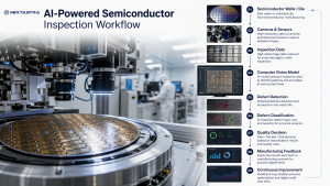
The important part is the complete system, not just the AI model. A production-ready solution also needs reliable image acquisition, data pipelines, model monitoring, deployment infrastructure, and integration with the manufacturing workflow.
That is where computer vision engineering and machine learning engineering have to work together.
Why False Positives Matter
One of the practical challenges in automated inspection is false positives.
An inspection system may identify something as a potential defect even when it is an acceptable variation. When this happens frequently, engineers have to spend time reviewing alerts that do not ultimately require action.
At high production volumes, this can create unnecessary review work and slow down the inspection process.
AI-based classification can help by learning patterns from inspection data and separating more relevant defects from less important variations.
The objective is therefore not simply to generate more alerts.
It is to generate more useful alerts.
Edge AI for Real-Time Inspection
Some manufacturing decisions need to happen quickly.
If every image or sensor reading has to travel to a centralized system before an inspection decision can be made, latency and data volume can become practical concerns.
Edge AI addresses this by running inference closer to the equipment generating the data.
This approach can be useful when a manufacturing system needs low-latency inspection, local processing, or rapid feedback.
The right architecture depends on the application. Some workloads may benefit from edge inference, while others are better suited to centralized or cloud-based processing.
Beyond Inspection: Other Uses of AI in Manufacturing
Inspection is only one part of the opportunity.
AI can also be used to analyze equipment and production data for predictive maintenance. Instead of waiting for equipment problems to occur, machine learning models can look for patterns that may indicate changing equipment conditions.
AI can also support process optimization by analyzing relationships between manufacturing parameters and production outcomes.
Another area is predictive quality, where production and inspection data are combined to identify conditions associated with potential quality issues.
These applications can work together rather than operating as isolated AI projects.
For manufacturing organizations, the bigger opportunity is creating a connected system in which inspection, equipment data, process information, and AI models contribute to the same operational picture.
Building Intelligent Semiconductor Manufacturing Systems
AI in semiconductor manufacturing is moving beyond individual automation tasks.
The direction is toward systems that connect:
Data + Computer Vision + Machine Learning + Edge AI + Manufacturing Operations
For example, an inspection system can detect a defect, classify it, send the result to a manufacturing system, and feed the outcome back into the data used to improve future models.
That creates a continuous cycle:
Detect → Understand → Decide → Improve
This is where AI becomes more than another software layer. It becomes part of the manufacturing process itself.
How NextAstra Approaches Industrial AI
At NextAstra, we work with AI, machine learning, computer vision, and data technologies to solve practical business and operational problems.
Our capabilities include computer vision, machine learning, real-time data processing, predictive analytics, and AI solutions for manufacturing.
For a manufacturing use case, the right solution may involve a single computer-vision model or a broader system connecting inspection data, machine learning, edge inference, and operational workflows.
The focus should always be the same: use AI where it can solve a real manufacturing problem and produce a measurable operational benefit.
Frequently Asked Questions
What is AI in semiconductor manufacturing?
AI in semiconductor manufacturing means using artificial intelligence and machine learning to analyze manufacturing, inspection, equipment, and process data. Common applications include defect detection, quality inspection, predictive maintenance, and process optimization.
How is AI used in semiconductor inspection?
AI can analyze inspection images to identify anomalies, detect defects, and classify inspection results. This can help manufacturing teams reduce unnecessary manual review and respond more quickly to important quality issues.
What is computer vision in semiconductor manufacturing?
Computer vision uses cameras and AI models to analyze visual information from manufacturing processes. It can support applications such as automated inspection, defect detection, and quality control.
What is edge AI in manufacturing?
Edge AI runs AI models close to the equipment or sensors generating the data. This can enable faster inference and real-time decisions where low latency is important.
Conclusion
Semiconductor manufacturing is becoming more complex, and the amount of data generated during production continues to grow.
AI can help manufacturers make that data more useful.
From computer vision and defect detection to predictive maintenance and edge AI, the opportunity is not simply to automate individual tasks. It is to build manufacturing systems that can detect problems, understand what they mean, and help teams respond faster.
That is the real potential of AI in semiconductor manufacturing.